TM 11-6625-444-14-1
Shift register flip-flop and zero gate
Subperiod
U1A
U2B
U4B
0..
ZERO
0......... 0.........
0.........
0...
.
.
....0
1.........
A. . . .
0......... 0.........
0.........
0...
.
.
....1
1 . . . . . . . 0.........
B...
0.........
0.........
0...
.
.
....1
0......... 1.........
0.........
C. . . . . . .
0.........
0...
.
.
....1
0 . . . . .... 0 . . . . . . . . .
0.. . . . . . .
1.........
0...
.
.
....1
D. . . . . . . .
0 . . . . 0.........
E....
0........
0.........
1...
.
.
....1
plied to the clock input of flip-flop U5B, are
k. The 16-state binary counter consists of J-K
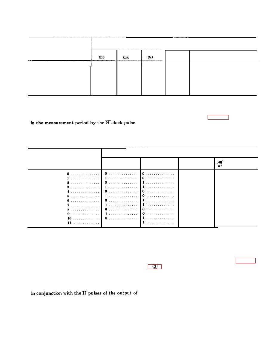
counted. The truth table for the flip-flops in the
flip-flop U5B, U5A, U6A, and U6B. The counter
binary counter is shown in table 5-3. The binary
is set to ZERO `at the beginning of each subperiod
counter is disabled by gate U2A if the count of 11
is attained.
During each subperiod of the digitizing cycle,
the output pulses from the CCO, which are ap-
Sixteen-state biary counter
Cco
pulse
count
USA
U5A
U5B
x
Z
Y
0
0...............
0
0...............
0
0...............
0
0...............
0
1...............
0
1...............
0
1...............
0
1...............
1
0...............
1
0...............
1
0...............
1
0...............
1...............
gating and control signals which are used to
control the synchronization of events in the
Q3. The CCO has no output until it is supplied
analog portion of the voltmeter, principally in the
cm-rent by the analog comparator and is enabled
A/D converter circuits. These signals, together
by the F output of J-K flip-flop U1B. The CCO
with other control signals, are shown in figure 5-
output is applied to the clock input of the 16-state
binary counter. T h e 9's catcher gate U7A,
NAND gates U8A through D, driving transistors
disables the CCO at a count of nine, if the
Q11 through Q17 and associated circuit elements.
volmeter is digitizing the second through fifth
o. The ladder switch driver circuitry (Q19
digits (subperiods B through E).
through Q22 on logic board) receives 8-4-2-1
m. The outputs of the six-state shift register,
coded binary data from the 16-state binary
counter and translates this to 4-4-2-1 coded
Q4, are applied to the display storage control
binary data, which matches the weighting of the
circuit consisting of transistors Q6 through Q10
and related components. Outputs from this
resistors in the ladder. Thus, the ladder output is
circuitry control the display storage circuit
proportional to the count in the binary counter.
The count increases until the output of the ladder
located on the A/D converter board (A9).
is sufficient to bring the A/D amplifier to the
n. The analog cycle control circuit produces the


