TM 11-6625-444-14-1
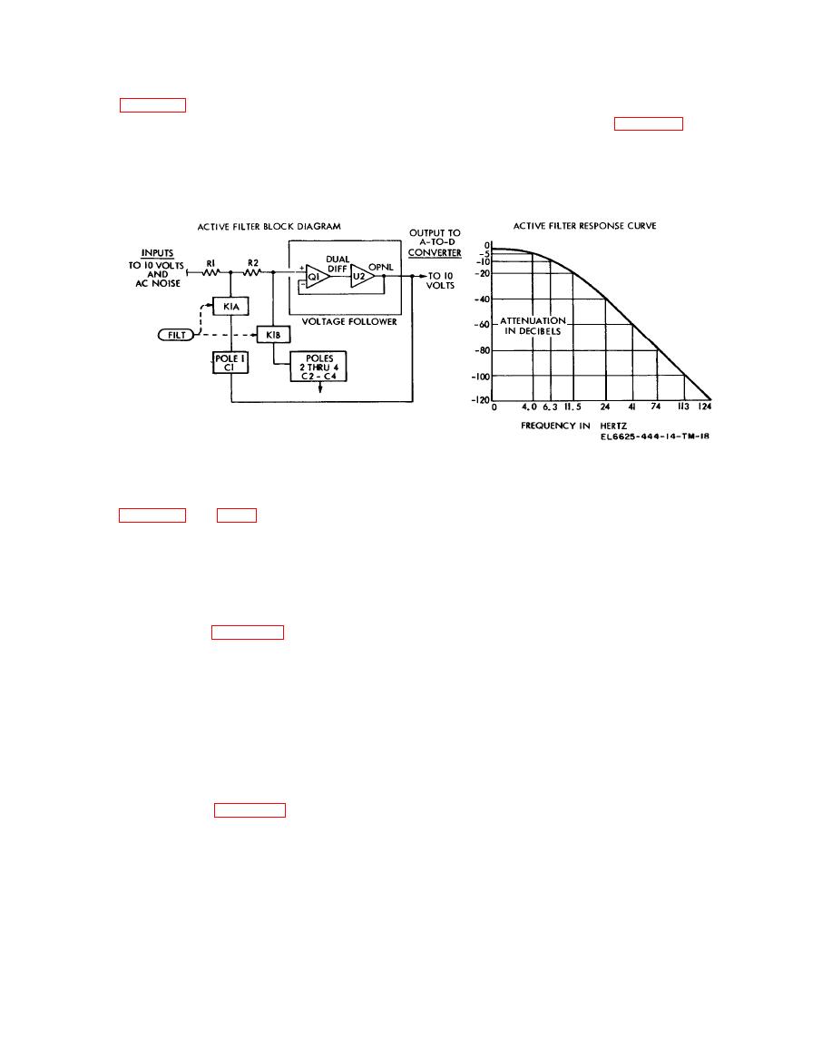
5-6. Active Filter
signal. Filtering occurs after the FILT button on
the front panel is depressed. A block diagram of
the active filter is shown in figure 5-3. Also shown
The active filter (A10) consists of a voltage
is the response curve of the active filter which
follower preceded by four poles of low pass
plots attenuation in decibels against a log scale of
filtering. These four poles attenuate undesirable
frequency in hertz.
ac signals which may be present in the dc input
5-7. A/ D Converter and Logic
input to the inverting amplifier during the C
subperiod.
(fig. FO-4 and FO-5)
c. The polarity detector consists of flip-flop
a. The A/D converter (A9) and logic circuits
Q10, Q11, and associated circuitry. The flip-flop
(A8) are discussed together in the following
employs base triggering, which is applied through
subparagraphs because any discussion of the
diode CR6 to the base of Q10. The gate signal,
analog-to-digital conversion process must include
gate 4, is applied to the emmitters of Q10 and Q11
elements of both circuits. The basic conversion
and enables the detector during the A subperiod
and logic circuitry involved in the conversion
of the measure period. During the remainder of
process in shown in figure 5-4. Also shown is an
the measure period, the plus and minus gates (Q8
arbitrary input voltage that is the equivalent to
and Q7, respectively) are turned off and the
the inverted, unknown voltage applied across the
polarity information is retained by the display
input jacks of the voltmeter. The output of the
converter is shown, applied to the following
stage, the display (A14) and consists of binary
Q20, operational amplifier U2, and associated
coded data bit groups that are serially emitted
components. Switch Q24 is turned on during the
from the converter and applied to the display
ZERO (0) sub period of the measurement period
circuits for decoding and serial display. The basic
by a ZERO signal from the logic circuit. This
purpose of the combined converter-logic circuitry
signal also controls switches Q19 and Q31, which
is to convert the analog voltage input (given as
are turned on during the ZERO subperiod to zero
+6.3524 dc volts in figure 5-4) serially by decade
the differential amplifier U2, and switch Q30,
to binary coded bit groups, one bit group per
which is turned off during the ZERO subperiod to
decade.
disconnect the amplifier output from the ladder.
Transistor Q29 and resistor R54 constitute a
s w i t c h Q3, dual FET input amplifier Q4,
clamp, which prevents amplifier U 2 from
operational amplifier U1, and associated cir-
saturating while its output is above 7 volts.
cuitry. Once every 18 milliseconds, during the
e. The analog comparator, c o n s i s t i n g of
subperiod, inverting amplifier switch Q6 is
t r a n s i s t o r s Q43, Q32, Q33, Q34, Q35 and
switched on by the inverting amplifier autozero
associated components, is basically a voltage
drive circuit in order to zero the inverting am-
comparator. Differential amplifier stage Q35
plifier. The drive circuit also supplies a turn-off
compares the A/D amplifier output with the +7
signal to transistor Q3, thereby removing the


