TM 11-6625-539-15-2
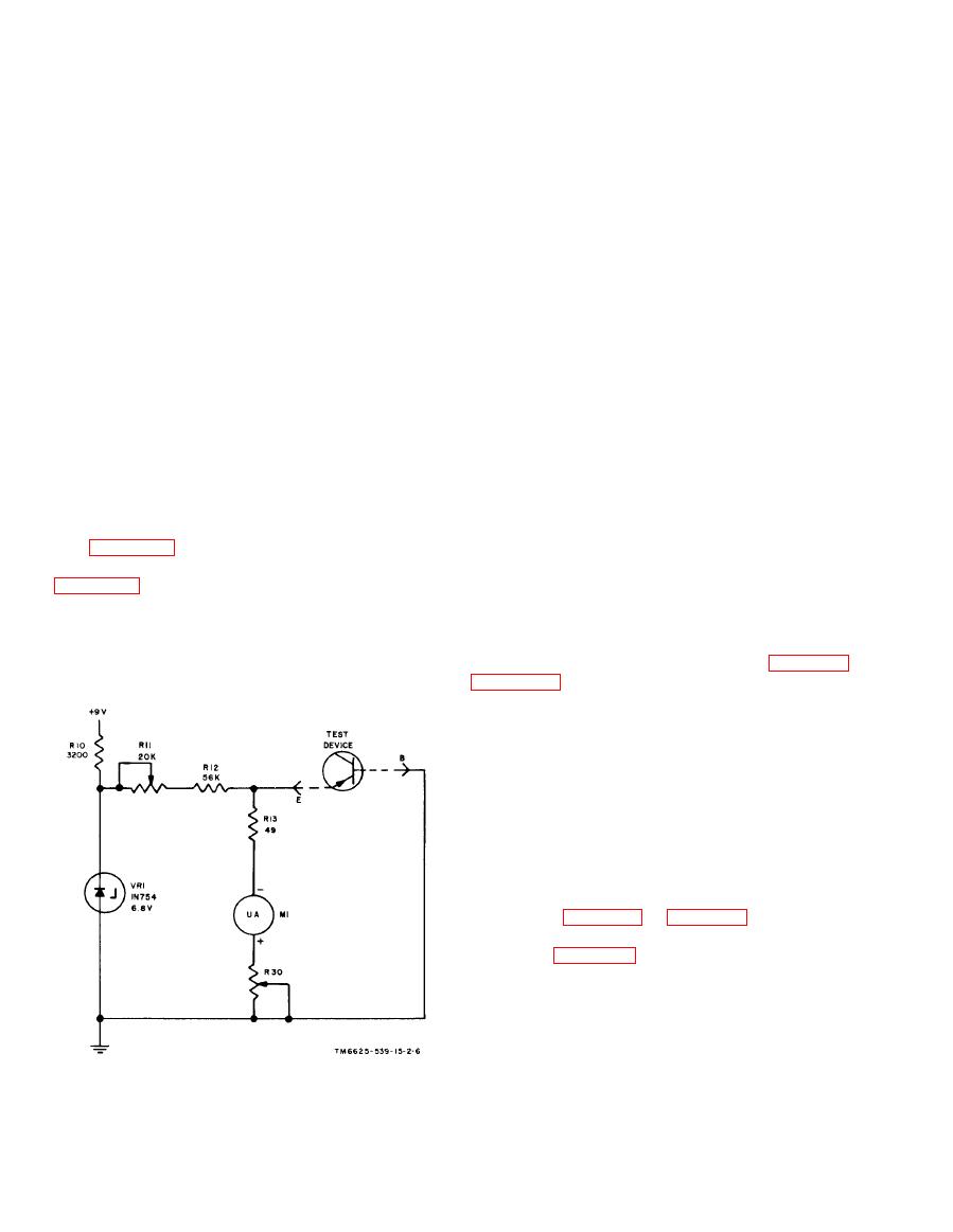
stant voltage source, eliminating the need for a meter
the same principle applies for NPN and four-element
zero potent iomet er. Resistors R11 and R12 limit the
devices ( tetrodes) when the fourth lead is left open-
maximum current through the meter to 100 ma. Re-
circuited.
sistor R11 is variable to compensate for tolerance var-
b. With the switch in the BETA CAL position, 1-
iations of the meter and resistor R13, which is in
kilohertz (kHz) multivibrator Q1, Q2, and Q3 ap-
series with the meter. Without the test device in the
plies a symmetrical square wave to the input of the
circuit, the full 100 ma flows through the meter, caus-
test device. The magnitude of the square wave is ad-
ing full scale deflection, which corresponds to a read-
justable by CAL resistor R5. The output of the square
ing of infinity. With the test device in the circuit,
wave generator is coupled to the test device by trans-
current flow through the test device, which is in-
former T1. With the switch in the BETA CAL posi-
versely proportional to resistance, results in a de-
tion, the amplitude of the square wave is adjusted
crease in current flow through the meter. Meter
by CAL resistor R5 until a 1-milliampere (ma) cur-
deflection in some amount less than full scale, depend-
rent flows in the collector of the test device. Setting
ing on the resistance of the test device, and indicates,
the function switch to BETA X1 connects meter
directly in ohms, the resistance of the element under
M1 to indicate the base current. Meter M1 is cali-
test. Because the test set measures semiconductor re-
brated directly in beta from the relationship beta
sistance at very low current and voltage levels, resist-
equals Ic/Ib, and beta is read directly. Setting the
ance at the semiconductor electrodes may be measured
function switch to BETA X10 removes shunt resistor
without polarizing the leads. The voltage used, 0.01
R27 from the meter, and the meter is 10 times as sen-
volt, is well below the knee of a voltage-current diode
sitive as in the BETA X1 position.
plot; consequently, the resistance of the diode is ex-
tremely high. The correct value of resistance is read
unless the diode is short-circuited or is excessively
Checks
leaky.
used to measure resistance of transistor junctions.
5-5. Leakage ICO X1 and X10 Check
measurements: however, the same principle applies to
A simplified schematic diagram of the circuit used
collector-to-base, and collector-to-emitter resistance
to check Ixco. (direct current (dc) collector current
measurements.
when the collector junction is reverse-biased and the
b. Resistor R10 and 6.8-volt Zener diode VR1 serve
emitter is open-circuited) is illustrated in figure 5-4.
as a voltage divider. Tile Zener diode establishes con-
function switch in the ICO X1 position, the test de-
vice is reverse-biased by the battery. The test device
emitter is open-circuited. Meter Ml indicates the col-
lector current. With function switch' at ICO X10,
shunt resistor R28 and series resistor R29 are con-
nected to the meter. The sensitivity of the meter is
decreased by 10.
5-6. DIODE 1-10 Ratio Check
a. A simplified schematic diagram of the circuit
used to check diodes for a 10 :1, front-to-back ratio
is shown on figure 55. A, figure 5-5, illustrates the
circuit used to obtain the forward or reference, read-
ing and B, figure 5-5, illustrates the circuit used to
obtain the reverse reading.
b. The 10:1 ratio measurement is obtained in the
following manner. The test device is placed in series
with the meter and its shunt and current limiting
resistors in both forward and reverse positions. With
the polarity switch in the FWD PNP position, the
Figure 5-3. Resistance check, simplified schcmatic diagram.


