TM 11-6625-539-14-4
EL6625-539-14-4-TM-6
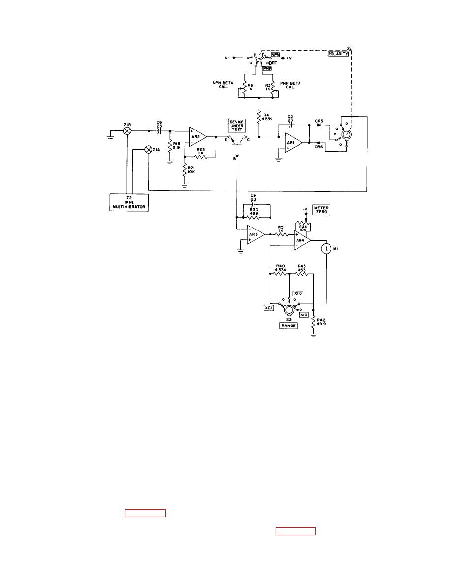
brator Z2 drives Z1A and Z1B, generating a
and drives the meter to a ratio proportional to RX
square wave at capacitor C6. The peak amplitude
and the range resistor.
of the square wave is equal to one-half the cali-
brated dc voltage at Z1A. The square wave is fed
b. The 10-mV voltage source for the ohms func-
into AR2 to provide a known calibrated signal
tion allows resistances to be measured without
level at the gate of the FET under test. The
forward biasing the function within the device
resulting drain/source current produces a signal
under test. The 10-mV output is well below the
level at resistor R1 which is coupled through
forward conducting level of both silicon and ger-
capacitor C11 to meter amplifier AR4. Amplifier
manium devices. Reliable circuit resistance will be
AR4 and diodes CR8, CR9, CR13, and CR14 pro-
indicated unless the device under test is shorted
vide an ac to dc conversion of the FET current to
or excessively leaky.
deflect the meter proportionately. Range resistors
R40, R42, and R43 adjust the signal to the re-
5-5. Field Effect Transistor (FET) Test Circuit
quired level to provide ranges of 250, 2,500, and
a. The FET test circuit simplified schematic
25,000 micromhos (microsiemens).
diagram is shown in figure 5-5. A calibrated dc
voltage divider consisting of resistors R7, R12, and
b. The circuit for an N-channel device is illus-
R14 feeds analog switch Z1A. The 1kHz multivi-
trated on figure 5-5. The circuit is identical for a


