TM 11-6625539-14-4
resistor is generated in that leg. This voltage is in
P-channel device, except that the polarity of drain
the direction to rebalance the bridge. The circuit
voltage is reversed at POLARITY switch S2.
is designed with values that cause the meter
deflection to be directly proportional to the ICES of
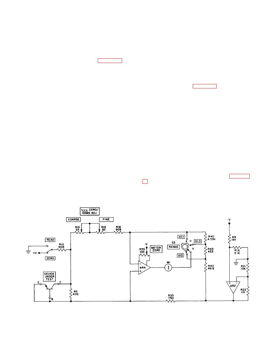
5-6. IC E S Function Test Circuit
the device under test. This balanced bridge tech-
nique cancels out all load resistances in the circuit
a. A simplified schematic diagram of the ICES
of the device under test.
function test circuit is shown in figure 5-6. The
test circuit uses a bridge circuit with the device
under test forming a part of one leg of the bridge,
5-7. I CO,IR Function Test Circuit
ICES ZERO/OHMS ADJ COARSE and FINE con-
a. The simplified schematic diagram for the ICO
trols R13 and R15 are also part of the bridge.
These controls are used to adjust the bridge to a
primarily a current-to-voltage converter. Ampli-
balanced condition when the ICES ZERO READ
fier AR2 and its associated components apply
switch is in the ZERO position. The bridge voltage
approximately 1.2 volts to the device under test.
is then changed to a lower value and rechecked
The resulting current flow-ICO for transistors, IR
for balance. If all legs of the bridge are purely
for diodes--is forced by amplifier AR3 to flow
resistive, the bridge will remain balanced under
through resistor R30, producing a voltage at AR3
all supply levels. However, if one leg contains an
that is proportional to the current flow.
element whose resistance is voltage dependent,
bridge balance will be upset as the supply
c h a n g e s . The I CES of a transistor is a current
b. The resultant voltage is fed into meter ampli-
constant independent of voltage, so that its equiv-
fier AR4 to produce through meter M1 a flow that
alent resistance is directly proportional to voltage.
is proportional to the leakage current of the de-
vice under test.
b. After the bridge is balanced using the ICES
ZERO/OHMS ADJ controls, the ICES ZERO READ
switch S4 is operated to READ. This lowers the
58. Diode In-Circuit Function Test Circuit
bridge supply voltage to approximately one-third
a. The simplified schematic diagram for the
diode in-circuit function test is shown in figure 5-
constant and unbalances the bridge. The unbalanced
condition is sensed by amplifier AR4 and the
output current drives the meter through range
presence of a semiconductor junction with as little
resistors R40, R42, and R43. A voltage that is
as 20 ohms in parallel. Transistors Q1 and Q2 and
proportional to the meter current and the range
amplifier AR2 with their associated components
EL6625-539-14-4-TM-9


