TM 11-6625-444-14-1
through CR13 and capacitor C8. The reference for
the external reference signal to a dc voltage
the +5 volts regulator is -18 volts. The series
between +0.7 to +7V dc. The difference am-
pass element is a compound-emitter follower
plifier consists of operational amplifier U7,
composed of transistor Q8 driving power tran-
resistors R1 through R12, and relay contacts K2A
sistor Q6. Voltage variation which are detected by
and B. The gain of U7 is 0.7, which is set through
the sample string (R14, R15 and R17) are am-
resistors Rl, R2, R3 and R4 with an external
plified by transistors Q7.
reference of 1 to 10.5V. Resistors R5 and R6
5-11. Ratio Input
parallel R4 when relay K2 is energized, thereby
changing the gain of U7 to 0.07 when the external
a. The ratio assembly (A3) supplies an internal
reference voltage is between +10.5 and 100V dc.
reference voltage from an external reference
Resistors R7, R8, R9, R10 and R11 and R12 are
source. Circuitry consists of a polarity detector, a
the reference leg for U7 positive terminal.
range detector, a difference amplifier, and a buffer
amplifier.
used to isolate the ratio input circuitry. The
b. The polarity detector applies a fixed polarity
buffer amplifier consists of FET Q5, operational
signal to the difference amplifier circuitry. The
amplifier U8, transistor Q6 and associated cir-
polarity detector consists of operational amplifier
cuitry. Transistors Q5 and Q6 control the input
U2 transistor, Q2, relay K1 and associated cir-
terminals of U8, R21, R23, and R24 which are
cuitry. The operational amplifier senses the
used in conjunction with R22 to correct an offset
polarity of the external reference signal and
voltage on the input terminals of U8.
controls the base voltage of Q2. Transistor Q2 will
f. R A T I O F U L L S C A L E p o t e n t i o m e t e r ,
activate relay K1 when the base is driven
transistors Q3 and Q4, provides a full scale ad-
positive. The signal at the external reference
justment of +50 and -50 digits in the readout.
terminals is applied to the difference amplifier
The conduction of Q3 is subsequently varied by
through the contacts of relay K1.
adjustment of the FULL SCALE RATIO control.
c. The range detector senses the external
5-12. Decimal Logic
reference voltage and conditions the difference
(fig. 5-7 and 5-8)
amplifier for operation in one of two ranges: 1V to
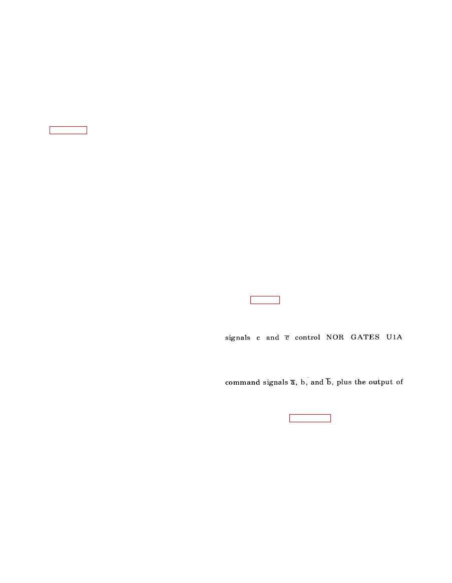
The purpose of the decimal logic assembly (A18)
10V; 10V to 100V. The range detector consists of
is to properly position the decimal in the readout.
operational amplifiers U1, U3, U4, U5, U6,
Transistors Q8 and Q9 and range command
transistor Q1 and relay K2 and associated cir-
cuitry. A portion of the external reference signal
through U1D so that two low signals appear on
is applied to the range detector circuitry through
the inputs to only one NOR GATE at a given
high impedance follower for isolation from the
time. The NOR GATE outputs are applied to
range detector circuitry. Amplifier U3 is wired as
transistors Q1 through Q7 and Q10. Range
a difference amplifier with a unity gain. Am-
plifiers U4 and U5 (combined) are an absolute
the NOR GATES, determine which transistor (Q1
value amplifier. The output of the absolute value
through Q7 and Q10) will be turned on, thereby
amplifer is equal to the input in value but is
controlling selection of which display tube will
always positive polarity whereas the input may be
display a decimal. Figure 5-7 is a truth table for
positive or negative. Operational amplifier U6
NOR GATES UIA through U1D and also shows
controls the base of Q1 which in turn controls the
conditions necessary to turn on Q1 through Q7
activity of relay K2. Relay K2 energizes when the
and Q.10.
external reference voltage exceeds 10.5 volts.
5-16


